Giter Club home page Giter Club logo

udb-c-legacy's Introduction

Unified Daughterboard Legacy C Series

Notice

The C3 series daughterboard has been deprecated with the launch of the C4 series.
This repository will be kept up for the sake of the ability to maintain legacy keyboards, but the legacy C3 daughterboard is now not-for-new-designs - please use the newer daughterboards instead for new keyboard projects.

In addition, documentation has moved to the new documentation site.


Original Readme

Introduction

The Unified Daughterboard Project is an attempt by leading designers in the mechanical keyboard community to standardize the USB daughterboards used for their custom mechanical keyboard projects. It has initially been envisioned by users ai03, Wilba, Hineybush, Xelus, Xondat, aeryxz and Maximillian.

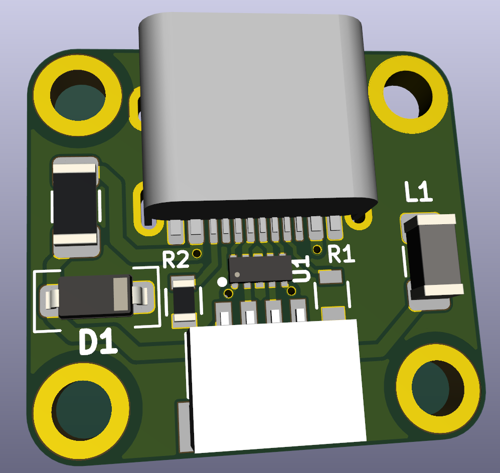
The main characteristic of this daughterboard is to integrate a USB Type C connector and the needed circuitry for USB2.0 operation in a small PCB that can be screwed to a keyboard chassis; this significantly simplifies the assembly and design of the main circuit board.

C3 version

In its current version, C3, this daughterboard features:

  • ESD (Electrostatic Discharge) protection on the data lines of the USB connector through a specialized chip;
  • Overcurrent protection through a PTC fuse;
  • Overvoltage protection through a bidirectional TVS diode;
  • Shielding noise decoupling capabilities through a ferrite bead;
  • Single-path grounding of the metallic chassis to which the daughterboard is attached.

Adittionally, the C3 version is backwards compatible with both C1 and C2 versions since it has the same dimensions and uses the same screw hole sizes and positions, so keyboards designed using the past versions should also support C3.

Detailed features

The figure below shows the schematic of the C3 version.

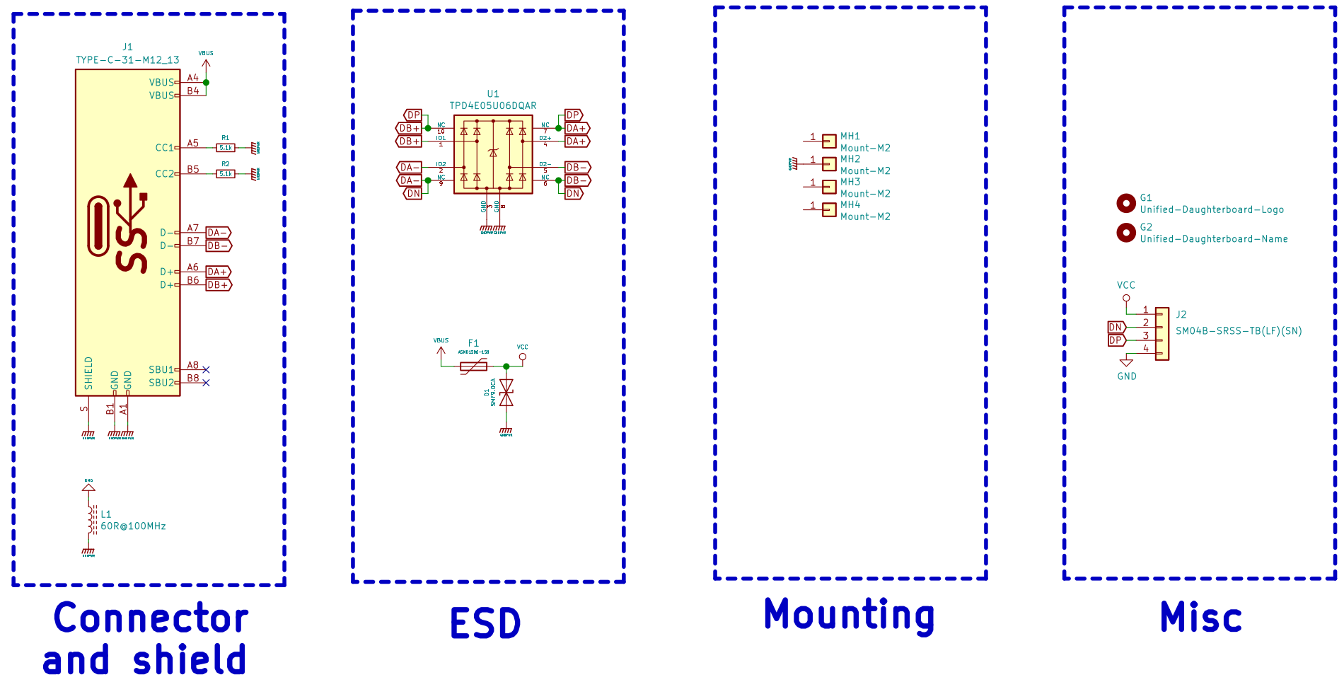
  • U1 is the ESD protection for the USB data lines. It is a ultra-fast, low-capacitance chip specifically designed for USB type C connectors. When one of the data lines presents a sudden voltage spike, this chip promptly grounds it -- avoiding damage to the circuit that uses these lines;
  • Resistors R1 and R2 are the CC resistors needed for operation of the USB Type C. These resistors are used by the USB host to know that the daughterboard is a downstream device and which side of the USBC connector is connected;
  • Fuse F1 provides overcurrent protection. It is a PTC resettable;
  • Diode D1 is a Transient Voltage Suppressor that exerpts to the power rails of the connector the same effect as the U1 chiup to data lines; when a voltge spike is detected, it shorts VCC and GND, aavoiding damage to the forward circuitry;
  • Inductor L1 is a ferrite bead that presetns a very low impedance between the power ground and the signal ground in DC regimen; in high frequencies (for instance in an ESD event) it presents a very high impedance, avoiding noisy currents passing to the signal GND;
  • The daughterboard features four screw holes used to fix it into a metal chassis. The top left mounting hole is shorted to the power ground signal; this means that the metal chassis of the keyboard will be grounded. However, the other three screw holes are not shorted to the power ground and are effectively isolated from that signal. This ensures that, in a discharge event emerging from the user providing charge to the system, the discharge current will have a single path through the daughterboard to the power ground; inductor L1 ensures that the discharge current is kept in the power ground plance and does not follow through to the signal ground.

Designer/Consumer info and references

Visit the docs

Previews

Render Render

Credits

udb-c-legacy's People

Contributors

ai03-2725 avatar gondolindrim avatar ramonimbao avatar

Stargazers

 avatar  avatar  avatar  avatar  avatar  avatar  avatar  avatar  avatar  avatar  avatar  avatar  avatar  avatar  avatar  avatar  avatar  avatar  avatar  avatar  avatar  avatar  avatar  avatar  avatar  avatar  avatar  avatar  avatar  avatar  avatar  avatar  avatar  avatar  avatar  avatar  avatar  avatar  avatar  avatar  avatar  avatar  avatar  avatar  avatar  avatar  avatar  avatar  avatar  avatar  avatar  avatar  avatar  avatar  avatar  avatar  avatar  avatar  avatar  avatar  avatar  avatar  avatar  avatar  avatar  avatar  avatar  avatar  avatar  avatar  avatar  avatar  avatar  avatar  avatar  avatar  avatar  avatar  avatar  avatar  avatar  avatar  avatar  avatar  avatar  avatar  avatar  avatar  avatar  avatar  avatar  avatar  avatar  avatar  avatar  avatar  avatar  avatar  avatar  avatar

Watchers

 avatar  avatar  avatar  avatar  avatar  avatar  avatar  avatar  avatar  avatar

udb-c-legacy's Issues

Add polyfuse for safe guarding board?

I'm kind of new to electronic/PCB work... I'm noticing on mostly all other repositories you have you advertise the overcharge + static charge protection, could this feature be added to this PCB?

EDIT: "other repositories" refer to your keyboard projects such as the Voyager series

It looks like the fuses rely on the gnd and vcc pins from the usb power (micro/C), so could this be added on a keyboard PCB file from the JST port?

PCB file might be corrupted?

๐Ÿ‘‹

First off thanks to all for making this open source!

Tldr' - When opening the PCB file in KiCad, I get the following error.
daughterboard

The weird thing is I have the latest version, 5.1.5 at the time of this writing.

======

Decided to start learning about PCB design; wanted to prototype something using a daughter board, came across this, looks perfect as is. Since I have 0 skill in SMD soldering nor the tooling I was hoping to get the fab house to assemble everything with parts. JLCPCB seems like the place to do it since they'll read everything off the gerber file and offer the service.

The issue is that for the assembly service, the project needs to be at a minimum 20x20 so I just wanted to tweak the edge cuts just a bit.

I cloned with --recursive so I believe I got everything, is there possibly something I'm still missing?

Also open to alternate places that could do the work, just looking at JLCPCB cause I've heard of em and they the easier interface to deal with.

Thanks so much ๐ŸŽ‰

Recommended future improvements

In reviewing the design of the Unified Daughterboard I found some room for improvements in future iterations of the design:

  • A bidirectional TVS is not ideal across the 5V rail, because it will permit a negative transient on VCC (such that VCC sees a negative voltage below GND). Better protection would be provided with a unidirectional TVS, as it would prevent VCC from being forced below GND.
  • The TVS in the BOM provides a min breakdown of 10V and a reverse standoff of 9V. This seems unnecessarily high for a 5V line.
  • Instead of having a discrete TVS, it seems like it would be optimal to make use of the existing ESD component on the board. It provides four channels of ESD protection, and there is no need for redundant ESD protection on the data lines. Recommend removing two of the redundant channels from the ESD I/O lines and using one of those channels to protect VCC instead. For an similar example of how this looks, see the datasheet for USBLC6-2SC6.
  • Ferrites are designed to filter out EMI in the >10MHz range. The intended use of a ferrite to restrict ESD currents will not be very effective, because the 8/20us ESD transient exists more in the 100kHz range where ferrites are still low impedance. Instead of using a ferrite for ESD purposes, it would be more effective for EMI purposes, by placing it between USB-C shield and USB-C GND connections, so as to provide higher impedance to the USB cable shield connection.
  • For metal keyboard cases (which are inherently susceptible to ESD discharges during normal use), there isn't really a great place to dissipate the discharge because USB devices typically don't have a direct path to earth ground (due to isolated power supplies upstream). Given that, that best option is simply shunt the discharge currents to the local ground, which will (harmlessly) cause the entire circuit potential to shift together during the transient. I mention this because it seems emphasized that the metal connection to case only goes through one mounting hole, which really doesn't benefit the circuit in any way. Whether it is tied to digital GND (or the USB shield) through one hole or four makes no difference.
  • If you really wanted to keep only one hole as conductive to the case, it would be better to remove the copper plane on the back of the board on those corner (or at least have them match the annular ring on the front). When making a mechanical connection to a metal surface, soldermask is not a reliable insulator; there are no inherent voltage withstand guarantees (noting however that the IPC standards do acknowledge some presumed voltage withstand capability), and soldermask is far to easy too accidentally scrape off during fastening.
  • The description states "when a voltge spike is detected, it shorts VCC and GND" which isn't quite accurate, in reality it just clamps the voltage (VCC or I/O line) to a safe level so as to prevent damage to other components.
  • It looks like there are a few instances of via-in-pad; this is not ideal for manufacturing as solder gets pulled into the via (unless you do a nonconductive epoxy fill), so yield may go down (or cost will go up).
  • A power trace on the back side immediately cuts underneath the data lines coming off the connector. Might be better for the USB signals if that trace were pushed up higher to be under the connector instead, giving a more consistent ground plane underneath. That said, I realize it will interfere with the star pattern in the copper, so...it may not be worthwhile?
  • USB signal traces aren't really the right width as per USB spec, but these traces are short enough that it might not matter. You'd probably need to go four layer to actually meet spec while keeping trace widths reasonable.

Recommend Projects

  • React photo React

    A declarative, efficient, and flexible JavaScript library for building user interfaces.

  • Vue.js photo Vue.js

    ๐Ÿ–– Vue.js is a progressive, incrementally-adoptable JavaScript framework for building UI on the web.

  • Typescript photo Typescript

    TypeScript is a superset of JavaScript that compiles to clean JavaScript output.

  • TensorFlow photo TensorFlow

    An Open Source Machine Learning Framework for Everyone

  • Django photo Django

    The Web framework for perfectionists with deadlines.

  • D3 photo D3

    Bring data to life with SVG, Canvas and HTML. ๐Ÿ“Š๐Ÿ“ˆ๐ŸŽ‰

Recommend Topics

  • javascript

    JavaScript (JS) is a lightweight interpreted programming language with first-class functions.

  • web

    Some thing interesting about web. New door for the world.

  • server

    A server is a program made to process requests and deliver data to clients.

  • Machine learning

    Machine learning is a way of modeling and interpreting data that allows a piece of software to respond intelligently.

  • Game

    Some thing interesting about game, make everyone happy.

Recommend Org

  • Facebook photo Facebook

    We are working to build community through open source technology. NB: members must have two-factor auth.

  • Microsoft photo Microsoft

    Open source projects and samples from Microsoft.

  • Google photo Google

    Google โค๏ธ Open Source for everyone.

  • D3 photo D3

    Data-Driven Documents codes.