Giter Club home page Giter Club logo

zerophone-pcbs's Introduction

Welcome to GitHub Pages

You can use the editor on GitHub to maintain and preview the content for your website in Markdown files.

Whenever you commit to this repository, GitHub Pages will run Jekyll to rebuild the pages in your site, from the content in your Markdown files.

Markdown

Markdown is a lightweight and easy-to-use syntax for styling your writing. It includes conventions for

Syntax highlighted code block

# Header 1
## Header 2
### Header 3

- Bulleted
- List

1. Numbered
2. List

**Bold** and _Italic_ and `Code` text

[Link](url) and ![Image](src)

For more details see GitHub Flavored Markdown.

Jekyll Themes

Your Pages site will use the layout and styles from the Jekyll theme you have selected in your repository settings. The name of this theme is saved in the Jekyll _config.yml configuration file.

Support or Contact

Having trouble with Pages? Check out our documentation or contact support and we’ll help you sort it out.

zerophone-pcbs's People

Contributors

crimier avatar dwaq avatar jaromir-sukuba avatar

Stargazers

 avatar  avatar  avatar  avatar  avatar  avatar  avatar  avatar  avatar  avatar  avatar  avatar  avatar  avatar  avatar  avatar  avatar  avatar  avatar  avatar  avatar  avatar  avatar  avatar  avatar  avatar  avatar  avatar  avatar  avatar  avatar  avatar  avatar  avatar  avatar  avatar  avatar  avatar  avatar  avatar  avatar  avatar  avatar  avatar  avatar  avatar  avatar  avatar  avatar  avatar  avatar  avatar  avatar  avatar  avatar  avatar  avatar  avatar  avatar  avatar  avatar  avatar  avatar  avatar  avatar  avatar  avatar  avatar  avatar  avatar  avatar  avatar  avatar  avatar  avatar  avatar  avatar  avatar  avatar  avatar  avatar  avatar  avatar  avatar  avatar  avatar  avatar  avatar  avatar  avatar  avatar  avatar  avatar  avatar  avatar  avatar  avatar  avatar  avatar  avatar

Watchers

 avatar  avatar  avatar  avatar  avatar  avatar  avatar  avatar  avatar  avatar  avatar  avatar  avatar  avatar  avatar  avatar  avatar  avatar  avatar  avatar  avatar  avatar  avatar  avatar

zerophone-pcbs's Issues

MCP_INT is push-pull on boot - expected open-drain, needs a PNP transistor in series

MCP23017, unexpectedly, has the INT pins in the push-pull mode on boot (at least it's still active low). This interferes with HAT EEPROM detection by Pi Zero, since it expects the GPIO0 to not be driven and instead pulled up to VCC. So, we need to add this solution between MCP23017 and Pi Zero/EEPROM:


Draft1.asc.txt

This also means we need to add a jellybean PNP transistor to the BOM. This is a suitable solution by now, but I'll look into whether we have a way around it.

Return the normal charging board placement

In Gamma version, I did a last-minute change to accomodate the new LiIon charging boards I got. That meant shifting the TP4056 breakout pinout out of the board outline, because the MicroUSB header was placed further than necessary. However, now it seems to me that sticking to more popular TP4056 breakouts (the ones that were used previously) would be a much better solution (not to mention that currently the breakouts used stick out of the board outlibe in a bad way, that'd interfere with case design.)

Alternatively, flipping the board could be considered - presumably, the heatsinking capability given by the soldermask opening on the board would be lost, but it could be not that big of an issue.

Diodes on keypad board

Currently, neither firmware nor hardware of the ZeroPhone keypad allow detecting more than one key at once. While the firmware is easier to adjust, the problem with hardware is that it doesn't have the diodes, which, AFAIK, are necessary for multiple simultaneous keypress detection. 1N4148 diode in MiniMELF is already used on the front board, so that component could be used here, too (possibly, in a smaller package).

Conversion to KiCAD5

Present project appears to be using KiCAD4 library structure. KiCAD5 changed this. Automatic migration not complete.

Request roadmap for toolchain upgrade

TPA2005 amplifier needs a ground pad on the footprint

Currently (Delta), the TPA2005 footprint center pad is not exposed. We need to add it, for better soldering possibilities, as well as in case the amplifier ends up heating up too much during, say, a loudspeaker cal

Lack of 3D models for many components

KiCad provides board 3D view/export functionality, which would be very useful for creating ZeroPhone cases. However, for many components used by ZeroPhone there just aren't suitable 3D models. What's necessary is to find/develop simple to-scale 3D models for these components and link them to the PCB so that they appear in the 3D viewer, and can then be exported by the KiCad VRML export option for case building. Most of the component size data can be gotten from footprints and ZeroPhone photos, and I'll post more component photos shortly for those components where dimensions might be unclear.

Changing through-hole pads to oval ones

In order to make ZeroPhone more reworkable, we need to make sure that pads stay on the board. @dwaq advice is:

In regards to the pad delamination, oval pads are typically stronger because there's more surface area, yet you can retain the spacing between the pins.

So, some of the through-hole pads should be made oval. I think it makes sense to do it for

  • GSM modem
  • front-to-keypad board connections
  • JST connector
  • USB port
  • Microphone

Possible but problematic places:

  • 40-pin Pi Zero headers (there are traces between them)

Places where holes can't/shouldn't be

  • Both 6-pin headers - there are traces going near them
  • Display header (8-pin and 7-pin holes are too close)
  • Audio jack footprint (the routing around it is cramped)
  • Expansion headers - not meant to be reworked (little use in reworking them), and not enough place

Powering the host USB port from charger voltage while ZeroPhone is charging

The USB step-up board is one of the only things that's powered from the battery even when the phone is charging (other things are GSM modem, IR expansion header, RGB LED and the MCP23017 expander). The problem is that, when there's a charger plugged in the USB port, IMO it makes sense to feed the charger input directly into the USB port. It could be done in different ways - a SPDT switch, a FET switch or something else. Waiting for comments and pull requests =)

A way to sense state of GSM hardware switch

As for now, the GSM hardware switch state can't be sensed from ZeroPhone. Thus, there isn't a way to distinguish between broken GSM modem (or the one whose firmware just crashed) and a GSM modem which was turned off in hardware. A GPIO from MCP23017 could be used for that, since there are still 5 left, but considering the comparator that could be added in the future revision, this needs more thought.

Front board: add ATMega RESET button footprint

A button could be useful for front board ATMega programming, in case somebody is assembling the ZeroPhone independently and doesn't have a USB-UART adapter with RESET line accessible.

3D model of TP4056 charger breakout

As I'm going to throw in quite some photos, I'm adding a new issue for the TP4056 board so that everybody who opens #12 doesn't have to load all the photos.

Board width
Board width
Board length - with MicroUSB port sticking out
Board length - without MicroUSB
Width of USB connector - without metal flaps
Width of MicroUSB connector - with metal flaps
Height of MicroUSB connector - with metal flaps
Height of MicroUSB connector - with metal flap
Height of MicroUSB connector - without metal flaps
Depth of MicroUSB connector
Distance from breakout top to back PCB top
Distance from breakout top to back PCB top - 3mm

PCB thickness - 1mm

JST connector for battery: P8 on back board

Making a new issue outside of #12 because this might get photo heavy again

I found this 3D model and I was attempting to add it to the board but it doesn't seem to match with the footprint.

I have it aligned in the X (x is up/down, y is left/right in this photo) direction, but need details on the Y direction. First off, does this appear to be the correct size? It's smaller than the outline in the X direction. In the Y direction, where should it align to? The edge of the PCB? If so, what set of holes do the pins fit? The ones nearest the PCB edge or the ones that are set further away? Some photos of the actual board might help me.
back_prototype

Silkscreen missing ESP-12 footprint pins

During assembly, a project's contributor was confused by missing ESP12 pins. Adding silkscreen ellipses where two deleted pins are would help eliminate this problem. Not sure KiCad supports it, though - worst case, I'll add two filled rectangles.

3D model of 5V DC-DC step-up breakout board

As I'm going to throw in quite some photos, I'm adding a new issue for the DC-DC board so that everybody who opens #12 doesn't have to load all the photos.

DC-DC PCB width
DC-DC PCB width
DC-DC PCB length
DC-DC PCB length

The inductor on the DC-DC has to be modelled, since it's a big part that interferes with other components. It would also be very helpful to actually see the 8-pin IC on the breakout - in case it could interfere with anything else, this is pretty much the second largest component.The IC is in SOIC-8 package and its model can be found in KiCad 3D model collection (for example, the same model is used for RTC IC on the bottom of the back board).
Height of the inductor
Height of the inductor from board surface to inductor top - 2.1mm
Inductor width and height
Inductor is a square, 6.5x6.5mm
Distance from board edge to inductor
Distance from board edge to inductor. In another dimension, the inductor is pretty much centered on the board, I think it's safe to assume it is.

Add fiducials to keypad boards

The keypad board is one of the boards that would benefit from fiducials the most. I forgot to include keypad board fiducials in Gamma release, but they have to be added - both to front and back of the board.

Adding comparators+reference for undervoltage detection

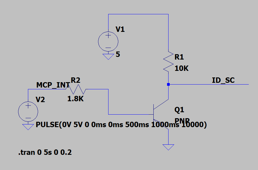
There are several undesirable hardware situations that need to be detected, that can't yet be detected by ZeroPhone. For example, the charging circuit can pull up to 1.5A from the charger. If the charger is not capable of providing that current, it will, possibly, drop the voltage and start overheating. It could also possibly mess with the LiIon charging board - while the chip used claims to work down to 4.0V (which in itself is weird, like, can you even charge a battery from this?), there's no guarantee the overloaded charger won't do some weird things. There are no free ADCs that could be used for determining whether the voltage is out of the bounds (there's one free ADC, but it's reserved for user applications), so technically a comparator could be used, using some free GPIOs on the MCP23017.

The 5V DC-DC chip used on the Chinese step-up breakout, while probably has some overload protection, has no way of notifying the user about output overload, while it could be very helpful while working with some USB devices. Again, a comparator could solve this.

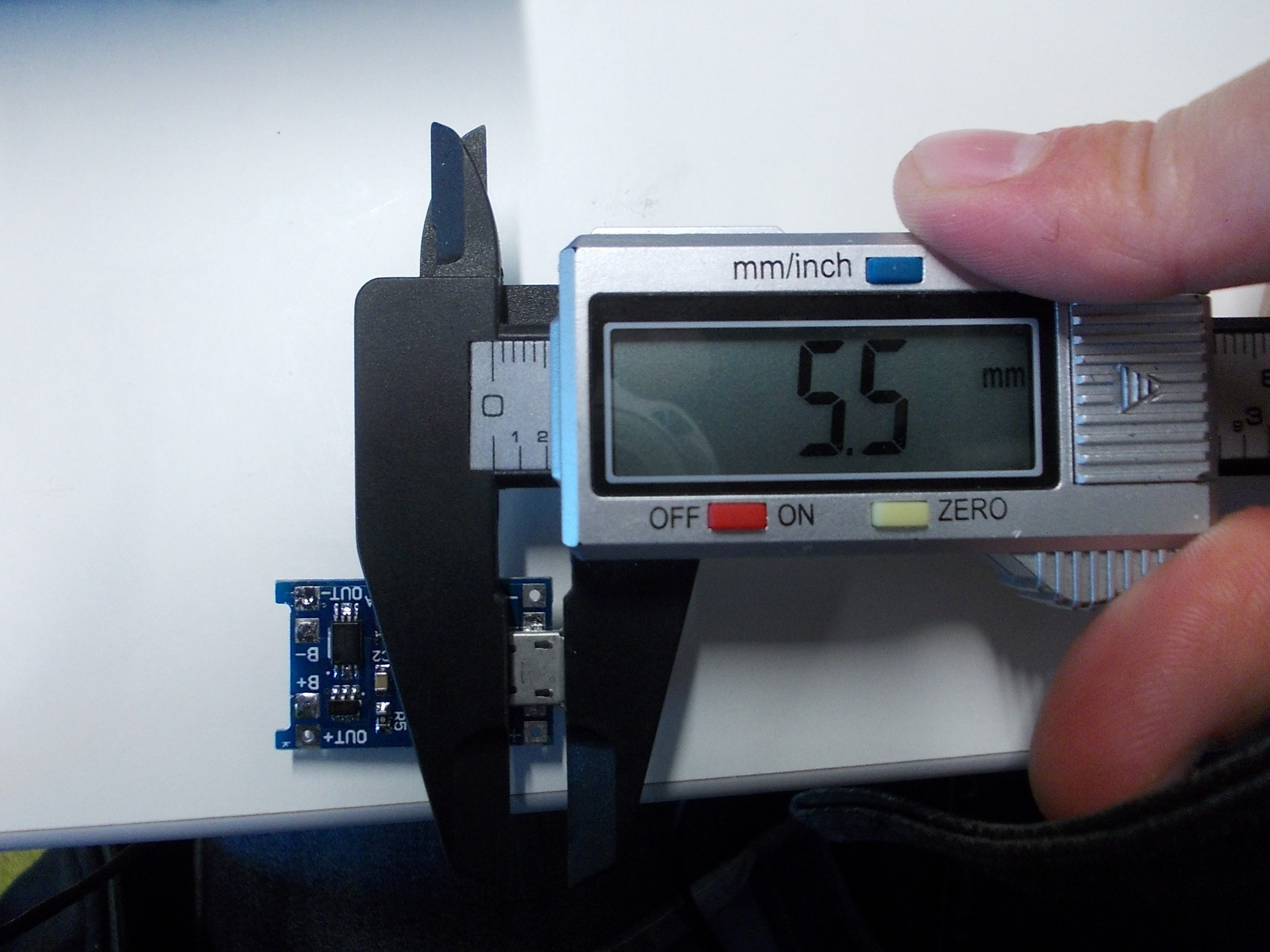
The battery is connected to the ATMega ADC and, with firmware allowing that, could be read by the Pi Zero through ADC. However, there's no hardware shutdown when the battery is lower than 3.0V - there's a protection circuit that shuts off at 2.5V, but I personally would like the cutoff voltage to be at least 3.0V. There's already a FET that cuts off VBAT in the current version of boards (Gamma), but it's only controlled from MCP23017, which, again, is controlled by software.

Also, some of the charger circuits are prone to going into some kind of thermal runaway when overheated (static discharge might play a role, too - at least I have no other explanation yet). They don't have to be put on the charger for this to happen - and if it happens, it's a bad thing, at best, the battery will discharge quickly. It's definitely a fault of the charger boards, but we still need to be able to detect it.

A solution I imagine would be using a quad comparator out of the popular ones, and having some kind of reference for it (that'd also be sourceable, solderable and cheap, just like the comparator has to be).

  • Charger input undervoltage monitoring
  • 5V output undervoltage monitoring
  • Battery charger circuit temperature detection - for a software warning
  • Battery charger circuit temperature detection - with a hardware cutoff of some sorts (higher temperature than the software warning temperature)

Move lower display header + fix SMD pads for display

As of now, when jumpering SMD pads to pins of the lower display header (as it's necessary to wire the display to signal pins on ZeroPhone), some solder goes into the plated holes and makes a small solder bulge, that, due to unfortunate positioning of the header, can short out to the OLED panel FPC pins. A temporary fix with Kapton tape can be used, but undesired as a requirement. So, this needs to be fixed in some way that doesn't involve post-processing
To add to that, unused pads could be removed from the footprint, to eliminate confusion. Also, silkscreen markings could really help avoid some costly mistakes, such as supplying reverse polarity voltage to the screen, destroying it in the process - though all the silkscreen additions probably warrant their own separate issue.

Back board - the ATMega header is hard to solder because of expansion headers

The back board has a 6-pin 2.54 header that's connected to the 6-pin ATMega programming/expansion header of the front board, and it's suggested to put a female socket on the back - so that the front board has a male header, which is easier to use for ATMega reprogramming However, currently the header holes are shifted in an awkward way, and the 6-pin header on the back board physically interferes with the 13-pin expansion header on the back board. My current solution is to file away the 6-pin female header with a file, but it's easier to just shift the 6-pin header to a lower position, which has to be done in the next version (breaking front-back board compatibility).

3D model of side button -

A datasheet can be found here, but I can't really find which button it applies to, and maybe that's not necessary. Basically, a block(base) (with somewhat flexible dimensions) plus block(button pin).

Pin dimensions:
Pin height
Pin height
Pin width
Pin width
Pin sticks out of the board outline by 0.4mm.

Swapping RGB LED for LED with digital controller

Currently, the RGB LED on the board is controlled by the MCP23017 GPIO expander. The expander doesn't support any kind of PWM, so right now it's only possible to show 7 colors on the LED.

Questions:
Are more than 7 colors really necessary?
What kind of LED could be used in place of a plain RGB LED?
What kind of peripheral could be used to drive that LED?

Adding silkscreen markings for onboard polarized capacitors

Currently, there's no clear designation of + orientation of the polarized capacitors on the boards. KiCad does have an asymmetric silkscreen, but it's confusing unless you explicitly look on where's the ground and where's the power connection. Waiting for pull requests =)

Move battery connector down ~1-2mm; SMD connector further into the board

Currently (Delta), a through-hole battery connector is interfering with the SIM5300EA breakout - by a really small margin, but it's going to be a bigger problem for the SMD connector. It only needs to be moved ~1-2mm down, so that it doesn't interfere with Pi Zero instead. Additionally, the SMD connector needs to be moved a little bit further into the board - to make sure the connector plug's body doesn't stick out of the ZP outline.

Switchover transistor and DCDC_EN FET can't coexist - need to add Schottky diode

The switchover circuit on Delta boards doesn't work as expected - the DCDC_EN is supposed to both control the FET that's switching the 5V DC-DC on and off, as well as the transistor that's enabling the switchover circuit. However, in practice, the transistor pulls DCDC_EN down when it's not yet configured as input - from the moment the phone (and MCP23017) is powered, till the moment the 5V DC-DC is first enabled/disabled (at that moment, the software sets the DCDC_EN GPIO as output). We could workaround that in software, but it's a hack. Instead, I came up with the following solution:

  • The transistor (that enables the switchover) is controlled from the charger input (through a 10K resistor) instead of DCDC_EN
  • A signal Schottky diode is added, pulling the transistor's base down whenever the DCDC_EN is low (and, consecutively, DCDC is enabled)

This enables the switchover when the charger is connected, but disables the switchover whenever DCDC is enabled.

The problem is - we need to add another BOM entry, as well as source another component. Therefore, if any other ideas are proposed, I'll be happy to hear them.

EOMA specifications and the future of ZeroPhone

I came across the FAQ on https://hackaday.io/project/19035-zerophone-a-raspberry-pi-smartphone/log/51834-explaining-choices-behind-the-project and wanted to mention, that there is a huge, more than 6 years running effort to:

  1. Create EOMA open-source specifications of interfaces for HW (not the HW itself), which build upon open-source and libre concepts, eco-consciousness, sustainability over many years, and affordability.
  2. Run a world-wide certification authority certifying compliance of devices with EOMA specifications.
  3. Boost spreading of EOMA specifications by manufacturing some HW made according to these interfaces specifications (see e.g. https://www.crowdsupply.com/eoma68/micro-desktop ).

For more information visit http://elinux.org/Embedded_Open_Modular_Architecture and http://rhombus-tech.net/ (it's messy, but it's getting better; so far use Ctrl+F on http://rhombus-tech.net/sitemap/ ). Except for desktop PC, notebook and tablet, there is also a phone. These links account for about 40% of information. The whole rest is scattered in the mailing list archives.

Some type of cooperation for the future ZeroPhone2 might be advantageous.

UART buffer addition

Currently, the Pi Zero UART (3.3V) is routed straight to the GSM UART (2.8V). The SIM800 datasheet advises against this, but fixing it would require quite some additional parts, such as a buffer of some kind, a voltage reference for 2.8V (since it's not exposed on the breakout). One more thing is that the same UART is, most likely, going to be used for the debug console - because there is just one UART, and debug console is a vital feature when doing low-level stuff and generally just debugging the reasons why system does not boot. So, theoretically, same buffer could be used for disconnecting the UART from the GSM modem - provided there's a free GPIO that could toggle the buffer, making sure that Linux boot data is not sent to the modem until the buffer is sent, and the boot console doesn't confuse the modem by printing lots of characters that may or may not contain something interpretable as AT commands. Ideally, the buffer could also be controlled by a small slide switch - so that you can signal the system not to turn the UART debug console off.

A suitable (easy to source, soldering-iron-solderable and cheap) buffer IC needs to be chosen, then added into the circuit, possibly using one of the GPIOs that are still free on the MCP23017.

Add UART pads near LiIon charging PCB outline

A mod board (replacement for LiIon PCB) can be developed, in order to have USB-UART access over the MicroUSB charging socket. For that, 1) a PCB with CP2102 and additional holes/castellations has to be developed 2) the UART traces (that go nearby) have to be brought to pads on PCB. The problem is that the debugging will be unusable when GSM modem will be active - but, considering the fact that there's already compatibility for both using UART as GSM modem comms channel and as a debug channel, this shouldn't be that big of a problem. Also, coupled with UART buffer addition (#6), a GSM modem-side override could easily be implemented, so that it'd be possible to use debugging console without modem receiving all the debugging info.

Possible audio problems and improvements

  • The DC blocking capacitor footprints (right before audio output) are meant to be 0805 and 1206 compatible. However, their pads are too close, even for 0603, so spacing the pads further away, and decreasing their size to maintain their current dimensions, might be necessary. (PCB needs to be printed out and measured)
  • The current audio circuit might benefit from a ground plane split in order to reduce interference (needs to be investigated)
  • 10pF and 33pF capacitors could be added on each channel in order to reduce the GSM frequency interference with the audio output
  • Currently, GSM speaker does not have a proper amplifier and the ringer is not very loud. We need to somehow amplify the sound - I've added a TPA2005 on Delta boards, but we will likely need a better solution.

Add a PCB identification EEPROM

The EEPROM could be used by zerophone_hw library and ZeroPhone UI, to identify between different versions of ZeroPhone PCBs. It's very likely to appear in the next version of PCBs, and will likely be added on I2C1 (user-accessible I2C), since I2C0 GPIOs are already taken by ESP8266 CH_PD and MCP23017 INT lines, and toggling them while OS is running could mean software breakage (mcp23x08 getting fake
interrupt signals, and esp8089 drivers suddenly losing the ESP8266 communication).

Changing via drill/annular ring size near pads to make rework less problematic

A friendly PCB designer made a comment from his experience - according to him, when there are components that are likely to be reworked, it makes sense to use larger vias and annular rings, so that, in case a PCB pad sticks off from PCB while reworking it, it would have a smaller chance of breaking off (to be fair, my memory fails me now). Rework on ZeroPhone boards would be necessary, for example, when trying out different displays, especially using the lower header (the one that has SMD pads for pinout selections).
Looking forward towards comments on whether it makes sense, as well as pull requests =)

Back board: R23 and Q1 interfere with certain charger boards

Certain charger&protection boards have "flaps" on the OUT side, because of a different panelization process (that some manufacturers use). We need to make sure those flaps don't interfere with aforementioned components - currently, those flaps would need to be cut away with tin snips.

Move the RGB LED up, to where it works better as a flashlight

The RGB LED, as placed on Gamma boards, needs some kind of light guide to be more useful as a flashlight, since it's covered by the 18650 holder. My proposition is: move it higher on the board and cut a corner off the 18650 board, so that it shines through (currently, the 18650 board has a cutout for the light guide, but the corner is intact).

Problems:

  • Some kind of light guide would still be useful - as, by default, the LED is quite diffused
  • We need to move a 100nF capacitor, which is there both for the top expansion port and for the LED.

RGB LED doesn't have polarity markings

Even though there are different 5050 LEDs with different polarities/pinouts, we need to mark the polarity for the LED version that we're suggesting (as well as add polarity disclaimer to the sourcing guidelines).

ATMega serial header reverse polarity protection

Connecting a USB serial adapter in reverse polarity appears to burn the ATMega328P (confirmed with 5V Arduino Serial Light - happens almost instantaneously). For now, users that want to reprogram their ATMega328P should be very careful about attaching the adapter the right way - future board revisions might need some way to prevent the damage from happening.

Comparator reference and inputs out of common mode range

LM339 has common mode range of 0V - Vcc-2V, which, for us, translates into 0V-1.3V. On Delta boards, everything is set up so that reference voltage is 2.5V (straight from TL431) and undervoltage triggers are around the same level, which is a mistake I let through because I didn't know about the fact there's a common mode range requirement. Suggested fix:

  1. Divide the TL431 voltage by 2 using a 10K-10K resistor divider
  2. Change the undervoltage resistor dividers in a way that divides the 4.6V trigger point into the TL431 voltage (approx. 1.25V)
  3. Adjust the thermocouple resistors accordingly (thermistor wasn't yet tested).

Needed silkscreen markings on PCBs

Front board:

  • Display SMD jumper pad connector pinout (#50)
  • Microphone polarity markings
  • SMD jumper pad configuration for the Heltek.cn display (likely to be the one used in production&kit versions) (#50)
  • Polarized capacitor polarity markings (given that most caps are tantalums, show a rectangle with a line corresponding to the line on capacitors, not just + sign) (#11)
  • ATMega programming header pinout (+warning about inserting the other way) (#46)
  • UART, VSYS and 4-pin keypad header pin names
  • Names for jumpers that can be cut/shorted (audio mod board overrides, ATMega GPIO mapping to 6-pin header, IR_RX/IR_TX)
  • R and C markings for 10K and 100nF, more detailed markings for elements with different values (put disambiguation somewhere)
  • For GSM filtering capacitor groups, add either "10pF" or "33pF" markings, depending on which are supposed to go where
  • More clear Pin 1 marking for ATMega

Back board:

  • Directions on soldering order: charging board first, then GSM modem, then 5V DC-DC, then USB port, then the USB testpoint wires and then the Pi Zero
  • Polarized capacitor polarity markings
  • Names for jumpers that can be cut/shorted (IR_RX/IR_TX, GSM power)
  • "Pull apart here" markings to see how to pull front board and back board apart
  • Expansion header pinout (possibly, better accomplished by stickers, for most headers)
  • "Hold to power" marking for FET override button
  • R and C markings for 10K and 100nF, more detailed markings for elements with different values
  • For GSM filtering capacitor groups, add either "10pF" or "33pF" markings, depending on which are supposed to go where
  • More clear Pin 1 marking for MCP23017

Keypad board:

  • Keypad row and column pin markings (for easier debugging)
  • Tips on soldering the keys

18650 holder board:

  • Version information
  • Battery polarity
  • First use instructions
  • 18650 battery handling warnings

Add small 6-pin header separator PCBs into main repo

There will be 2 6-pin headers linking the back and front boards (right now, one of them is 4-pin but it'll be changed). When Pi Zero is soldered on the back board, however, there's a 1.6mm offset, which needs to be compensated for by a spacer, and a piece of 1.6mm PCB seems to be the most suitable material. In addition to that, the PCB might also work as a holder for the GSM antenna wire (so that it doesn't obstruct the miniHDMI connector).

3D model of display

As I'm going to throw in quite some photos, I'm adding a new issue for the display so that everybody who opens #12 doesn't have to load all of them.

Total screen width
Total screen width
Total screen height
Total screen height
Margin from PCB top to panel top
Margin from PCB bottom to panel bottom
Panel height
Panel height
Panel width
Panel width
Panel bottom non-active area height

On back board, ATMega header is reversed

GND pin is supposed to be on other side of the header - so the header needs to be rotated 180 degrees. This means that ATMega analog port is not correctly routed to the header in Gamma PCB version.

Recommend Projects

  • React photo React

    A declarative, efficient, and flexible JavaScript library for building user interfaces.

  • Vue.js photo Vue.js

    🖖 Vue.js is a progressive, incrementally-adoptable JavaScript framework for building UI on the web.

  • Typescript photo Typescript

    TypeScript is a superset of JavaScript that compiles to clean JavaScript output.

  • TensorFlow photo TensorFlow

    An Open Source Machine Learning Framework for Everyone

  • Django photo Django

    The Web framework for perfectionists with deadlines.

  • D3 photo D3

    Bring data to life with SVG, Canvas and HTML. 📊📈🎉

Recommend Topics

  • javascript

    JavaScript (JS) is a lightweight interpreted programming language with first-class functions.

  • web

    Some thing interesting about web. New door for the world.

  • server

    A server is a program made to process requests and deliver data to clients.

  • Machine learning

    Machine learning is a way of modeling and interpreting data that allows a piece of software to respond intelligently.

  • Game

    Some thing interesting about game, make everyone happy.

Recommend Org

  • Facebook photo Facebook

    We are working to build community through open source technology. NB: members must have two-factor auth.

  • Microsoft photo Microsoft

    Open source projects and samples from Microsoft.

  • Google photo Google

    Google ❤️ Open Source for everyone.

  • D3 photo D3

    Data-Driven Documents codes.