Giter Club home page Giter Club logo

8bit-cpu's Introduction

MK1 8bit Computer

Schematics and code for my home-made 8-bit CPU and its companion boards.

Articles about this project:

Hackaday.com

Hackster.io

InformaticaLab.com

Overview

During the past month, I designed and built a programmable 8-bit CPU from scratch, out of basic series 74LS logic ICs.

This repository contains pictures, schematics, and code for this project and its companion boards.

  • V 1.0 assembled:

  • V 2.0b assembled:

  • Helix Display Interface in action:
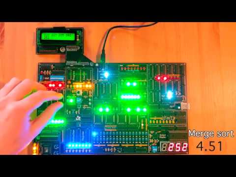
  • V 1.0 in action:

DEMO VIDEO (YouTube)

MK1 Computer - home-made Programmable 8bit CPU

Architecture

The MK1 CPU is composed of several modules, all connected trough a common 8-bit BUS, the status of each module is shown by dedicated LEDs.

  • The clock module is designed to allow step-by-step execution; in automatic mode the clock speed can be adjusted from 1Hz up to 32KHz.
  • The computer programs are stored in RAM and the CPU can be programmed both manually, by inserting binary machine code through dip-switches, and automatically via a USB PC interface.
    • The Programming interface is designed to be used in conjunction with an Arduino Nano or the Start9 programming board.
    • The Start9 programming board allows the loading of multiple programs stored on an on-board flash memory without the aid of an external computer device.
  • The Addressable memory space is 1024 byte, data, stack and code spaces are separated, the code address space is not writable.
  • The instructions are variable-length (see instruction-set here) 1 or 2 bytes long (first byte for the opcode, the second one for the argument), there are 4 general purpose registers (A, B, C, D) and a stack pointer register for subroutine calls.
  • The Arithmetic Logic Unit has a dedicated register for the second operand and supports the following operations:
    • Addition
    • Subtraction
    • OR
    • AND
    • NOT
    • Left/Right Shift
    • Left/Right Rotation
  • The Control Unit combinatory logic is implemented using EEPROMs (see microcode here) whilst each instruction is realized through a variable number of micro-instruction for a maximum of 6 micro-steps per instruction, including the fetch cycle. The instruction-set supports both direct and indirect memory access as well as absolute and conditional jumps on carry (CF) and zero (ZF) ALU flags.
  • The computation output can be visualized on a 4-digit display, with a dedicated register, able to represent positive and 2-complement negative numbers both in decimal and hexadecimal format.
  • The CPU can be extended thanks to the external BUS interface capable of handling up to 2 peripheral. The communication is bidirectional, the devices can send interrupts to the CPU to notify when new data is available. Interrupts are cleared once the data has been processed.
    • The only available peripheral at the moment is the Helix display interface, an ATmega328-driven 2x16 LCD output display.

Structure

  • MK1 CPU/:
    • 8bit-computer/: KiCad project, schematics and PCB design of the MK1 CPU.
    • code/:
      • microcode.py: generates the binary EEPROM microcode.
      • out_display.py: generates the binary output display EEPROM code.
      • uploader.py: uploads a binary MK1 program to the CPU.
      • mk1_computer_uploader/: Arduino programmer interface sketch.
    • assembler/: fork of the hlorenzi's assembler, improved and customized for the MK1
    • programs/: a collection of programs for the MK1 CPU plus the assembler definition
  • start9_programming_interface/:
    • programming_interface/: KiCad project, schematics and PCB design of the Start9 programming board.
    • code/start9_programming_interface/: Arduino code for the programming interface.
  • helix_display_interface/:
    • display_interface/: KiCad project, schematics and PCB design of the Helix display interface board.
    • code/helix_display_interface/: Arduino code for the display interface.
  • eeprom_programmer/: KiCad project, schematics and PCB design of a simple Arduino-based eeprom programmer
  • bus_breakout/: KiCad project, schematics and PCB design of the external bus connector breakout board.

Changelog

V2.0d:
  • minor hardware revision
  • revisited PCB design
  • new memory architecture, code memory section is read-only, stack and data live on separated spaces
V2.0b:
  • minor hardware revision
  • Variable-length instructions (1 or 2 bytes)
  • new custom assembler, thanks to https://github.com/hlorenzi/customasm
  • few new instructions
  • revisited microcode and instruction-set
V2.0:
  • 4 general purposes registers (A, B, C, D)
  • Stack Pointer implemented as an up-down counter
  • External interface and interrupt handling
  • Output display decodes HEX and ASCII values
  • Clock speed multipliers
  • Control Unit extended with 4 EEPROMs
  • Variable step microcode counter length (each instruction uses the minimum amount of micro-steps)
  • revisited microcode and instruction-set
V1.0:
  • Bugfixes.
  • HL and STK address signals available in the MAR dip-switch.
V0.1:
  • Initial release

8bit-cpu's People

Contributors

vascofazza avatar

Stargazers

 avatar  avatar  avatar  avatar  avatar  avatar  avatar  avatar  avatar  avatar  avatar  avatar  avatar  avatar  avatar  avatar  avatar  avatar  avatar  avatar  avatar  avatar  avatar  avatar  avatar  avatar  avatar  avatar  avatar  avatar  avatar  avatar  avatar  avatar  avatar  avatar  avatar  avatar  avatar  avatar  avatar  avatar  avatar  avatar  avatar  avatar  avatar  avatar  avatar  avatar  avatar  avatar  avatar  avatar  avatar  avatar  avatar  avatar  avatar  avatar  avatar  avatar  avatar  avatar  avatar  avatar  avatar  avatar  avatar  avatar  avatar  avatar  avatar  avatar  avatar  avatar  avatar  avatar  avatar  avatar  avatar  avatar  avatar  avatar  avatar  avatar  avatar  avatar  avatar  avatar  avatar  avatar  avatar  avatar  avatar  avatar  avatar  avatar  avatar  avatar

Watchers

 avatar  avatar  avatar  avatar  avatar  avatar  avatar  avatar  avatar  avatar  avatar  avatar  avatar  avatar  avatar  avatar  avatar  avatar  avatar  avatar  avatar  avatar  avatar  avatar  avatar  avatar  avatar  avatar  avatar

8bit-cpu's Issues

* on PCB Layout

I am currently building the 2.0d, and I see some * on the PCB layout and BOM. What are these supposed to be?
Thanks!

Opcodes that can be repurposed

This is not a bug and not yet a feature request, more intended as discussion and preparation for expansion if the author or any other folks looking at this project want to collaborate on this part.

The existing code already fits exr, exw, j*, cmp, not, sll, slr, rll, rlr, hlt, and add/sub/or/and imm into some of the gaps where the larger opcode patterns would be meaningless or close. I am looking at the instruction set and opcode list and considering where more instructions can be squeezed in. Akin to my previous post, I apologize in advance if I've gotten anything wrong. I've started putting together the parts list to build a version of this computer, but it's going to be a while before I have hardware to play on.

Here are my notes:

load $x [$out] is already repurposed for $a and $b. The other 5 destination registers are ripe for the taking, at no cost.

move $x $x is a nop. It's so nop that nop maps to move $a $a, and so could all of them. Since move imm, imm is already reclaimed and we need to keep one to cover all of them, this would open up 6 opcodes at no cost.

move $out $x isn't valid because the output register is write-only. This would open up 7 opcodes (6 if you already got one from the previous line).

and/or $x $x sets zf if $x is 0, clears cf. I think that add 0 $x would do the same, at the cost of 1 step. This would open up 8 opcodes.

stor $x, [$pc] is a quandary. The readme for the project says program memory (HL, bytes 0x100 to 0x1FF, I think?) isn't writable, but I don't see that implemented in the current schematic. If it works, it could only write to the next instruction to be executed, which seems of very limited use. I suspect this can be given up to gain 4 more opcodes.

load $x, [$pc] seems only slightly more useful. Reading only the next instruction from program memory might enable some specific clever trick, but I don't see it. I'd also give this up for 4 more opcodes.

sub $x $x sets $x to 0, sets zf, clears cf. I think that cmp $x; ldi $x 0 does the same for $b/$c/$d, and ldi $a 0; cmp 0 for $a, at the expense of one byte of code and 3 clock cycles. This would open up 3-4 opcodes.

That's about 20-35 opcodes available for additional instructions depending on priorities. I have ideas for what to do with them, but that's probably a subject for another discussion. Whether there's agreement or not on what to do with them, it would be useful to have some agreement on which existing opcodes to repurpose, for maximum compatibility between programs in the future. My preference would be to start at the top of this list.

Helix Display LCD

Could you provide the name of the LCD Display used with the Helix Display Interface? I am struggling to find one with the correct pin layout.

Problems with `ldi reg 0`

I should preface this by saying that I haven't built your computer yet, but I want to, either in a simulator or on breadboards, and I prefer to dive into the repository and code before getting physical. So, I'm sorry if some (or, hopefully not, all) of my "will" and "should" below are inaccurate or off base.

ldi {dst: reg} 0 => 0b11 @ 0b01 @ 0b00 @ dst[1:0]

This seems to convert ldi $a 0 into 0b11 01 00 00 which microcode.txt tells me is equivalent to sub $a $a instead of the move 0 $a that I would otherwise expect. While that instruction will produce the clearly desired effect of putting 0 into the a register, I think there are a few problems with this:

  1. sub sets flags while move does not. That means ldi $a 0 will set the zero flag, but ldi $a 1 will not clear the zero flag. As a programmer, this is not behavior I would expect or desire.
  2. ldi $b 0 is converted to 0b11 01 00 01 which is sub $a $b. Should the third crumb 0b00 here be another dst[1:0] instead so that this will produce 0b11 01 01 01 or sub $b $b?
  3. Both sub reg reg and move imm reg take 4 steps. This optimization saves a byte of code, but costs some power activating a bunch of extra control lines and circuits.
  4. dst[1:0] truncates the dst parameter to 2 bits, so ldi $sp 0 is accepted by the assembler and produces identical machine code to ldi $a 0, and ditto for $pc/$b and $out/$c. This line should include { assert(reg <= 4) ... } or equivalent.
    This concern also applies to {op: alu_op} {operand_1: reg} {operand_2: reg} => 0b11 @ op[1:0] @ operand_1[1:0] @ operand_2[1:0]
  5. No example programs use this pattern for any register other than a. The test suite program doesn't use it at all. Every separate line in the assembler definition probably deserves at lease one test case.

I hope at least some of this makes sense and is helpful.

Version control w/ example code and customasm syntax

Hi there,

As best I can tell there seem to have been some hugely backward-incompatible changes to customasm since the original (very well written!) examples were uploaded. I've tried and failed to port the definitions to the current expectations of customasm and failed, probably in equal parts due to my unfamiliarity with both customasm and the mk1's instructions. It's a pity, I was looking forward to making a pull request! This addresses some but not all of the issues, and having applied each of these suggested migration changes we're still in a bad way - for example I see nothing about migrating the ' marks contained in the existing instruction definitions (e.g. "3'5"), they look like they could be slice notation but no joy there.

There seems to have been a shift away from 'cpudef' and 'tokendef' (although it looks like the parser still honours both so this is the least of all issues), the bankdef syntax no longer allows/requires quotation marks but even once that's fixed it throws panics due to the overlap in the two banks' respective locations. The thing I've totally failed to understand the root of - as your syntax looks identical to Lorenzi's to my eye - is casm's dislike of the way your registers and ALU opcodes are set out, and to every reference thereafter containing a $ sign.

Finally and somewhat bizarrely I can't even seem to find a historical build from ~2019 that likes the example code, so I'm not sure what's going on there either.

Regards,

Greg

Programming AM29F040

Hi there, how did you go about programming the AM29F040 flash memory? I have built the eeprom programmer but from what I can tell that is setup to program the EEPROM handling the 7 segment leds. I am unable to find a good example of how to program the AM29F040 online. Your help is greatly appreciated!

Programming Interface

Could you please explain how to program the programming interface? I am a little confused as to what the arduino code start9_programming_interface.ino and the flash_composer are meant to do. Also, how does flash composer communicate with the a pc? Sorry for so many questions, I am just trying to follow the build and need a little assistance. Thank you!

Unexpected Behavior (Clock, Reset, Programming Interface)

Hi! I believe I have been able to successfully program the Flash as well as the ATMega for the programming interface, but I am unable to understand why I am getting the results I am currently. Here is a video of what I have so far: https://imgur.com/a/B3an2lI

As you can see in the video, one of the first issues is that the clock doesn't seem to work. When I try to switch it on, nothing seems to happen. The pulse button does work (sometimes).

The next issue is that the reset button for some reason doesn't clear the C register.

And finally, the programming interface doesn't do anything (from what I can tell), since none of the LEDs are lighting up indicating it is programming.

Do you think that these issues could all be caused by incorrect programming of the AM29F040Bs? I was able to use the FMPUno and it seemed that they were programmed correctly when I read the contents.

Recommend Projects

  • React photo React

    A declarative, efficient, and flexible JavaScript library for building user interfaces.

  • Vue.js photo Vue.js

    ๐Ÿ–– Vue.js is a progressive, incrementally-adoptable JavaScript framework for building UI on the web.

  • Typescript photo Typescript

    TypeScript is a superset of JavaScript that compiles to clean JavaScript output.

  • TensorFlow photo TensorFlow

    An Open Source Machine Learning Framework for Everyone

  • Django photo Django

    The Web framework for perfectionists with deadlines.

  • D3 photo D3

    Bring data to life with SVG, Canvas and HTML. ๐Ÿ“Š๐Ÿ“ˆ๐ŸŽ‰

Recommend Topics

  • javascript

    JavaScript (JS) is a lightweight interpreted programming language with first-class functions.

  • web

    Some thing interesting about web. New door for the world.

  • server

    A server is a program made to process requests and deliver data to clients.

  • Machine learning

    Machine learning is a way of modeling and interpreting data that allows a piece of software to respond intelligently.

  • Game

    Some thing interesting about game, make everyone happy.

Recommend Org

  • Facebook photo Facebook

    We are working to build community through open source technology. NB: members must have two-factor auth.

  • Microsoft photo Microsoft

    Open source projects and samples from Microsoft.

  • Google photo Google

    Google โค๏ธ Open Source for everyone.

  • D3 photo D3

    Data-Driven Documents codes.